على الرغم من صعوبة معالجة ركيزة كربيد السيليكون ، إلا أنه من أجل جعل تطبيق كربيد السيليكون البلوري الفردي في المكونات الإلكترونية هو الاتجاه المستقبلي للتنمية، بحيث تصبح أجهزة كربيد السيليكون تطبيقًا وترويجًا على نطاق واسع، ومن الضروري إيجاد طريقة لحل مشكلة صعوبة معالجة كربيد السيليكون.
في الوقت الحاضر، تشتمل تكنولوجيا معالجة المواد SiC بشكل أساسي على العمليات التالية: القطع الاتجاهي، والطحن الخشن للرقاقة، والطحن الدقيق، والتلميع الميكانيكي، والتلميع الميكانيكي الكيميائي (التلميع الدقيق). من بينها، التلميع الكيميائي والميكانيكي هو العملية النهائية، ويؤثر اختيار طريقة العملية وترتيب مسار العملية وتحسين معلمات العملية بشكل مباشر على كفاءة التلميع وتكلفة المعالجة.
ومع ذلك، نظرًا للصلابة العالية والاستقرار الكيميائي لمواد SiC، فإن معدل إزالة المواد في عملية التلميع التقليدية CMP منخفض. ولذلك، بدأت الصناعة في دراسة تكنولوجيا الكفاءة المساعدة التي تدعم تكنولوجيا التصنيع فائقة الدقة، بما في ذلك بمساعدة البلازما، بمساعدة المحفز، بمساعدة الأشعة فوق البنفسجية ومساعدة المجال الكهربائي، على النحو التالي:
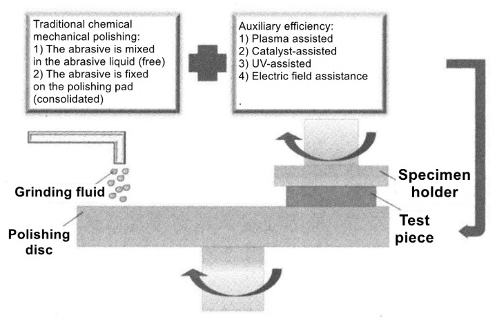
01 تقنية البلازما المساعدة
يامامورا كازوي وآخرون. اقترح لأول مرة عملية التلميع بمساعدة البلازما (PAP)، وهي عملية تلميع كيميائية ميكانيكية مساعدة تعمل على أكسدة المواد السطحية إلى طبقة أكسيد أكثر ليونة من خلال البلازما، مع الاستمرار في إزالة المواد عن طريق الاحتكاك الكاشطة والتآكل.
المبدأ الأساسي هو: من خلال غاز تفاعل مولد الترددات اللاسلكية (مثل بخار الماء، O، وما إلى ذلك) لإنتاج بلازما تحتوي على مجموعات حرة (مثل مجموعات OH الحرة، O الجذور الحرة)، مع قدرة أكسدة قوية للمجموعات الحرة على سطح تعديل أكسدة مادة SiC. يتم الحصول على طبقة أكسيد ناعمة، ومن ثم تتم إزالة طبقة الأكسيد عن طريق التلميع باستخدام مواد كاشطة ناعمة (مثل CeO2، Al2O3، وما إلى ذلك)، بحيث يصل سطح مادة SiC إلى المستوى الذري للسطح الأملس. ومع ذلك، نظرًا لارتفاع أسعار معدات اختبار عملية PAP وتكاليف المعالجة، فإن الترويج لرقائق SiC لمعالجة عملية PAP محدود أيضًا.
02 عملية بمساعدة المحفز
في المجال الصناعي، من أجل استكشاف تكنولوجيا التصنيع فائقة الدقة وعالية الكفاءة للمواد البلورية SiC، يستخدم الباحثون الكواشف للتلميع الكيميائي والميكانيكي بمساعدة الحفاز. الآلية الأساسية لإزالة المواد هي أن طبقة الأكسيد الناعمة تتشكل على سطح SiC تحت تحفيز الكواشف، وتتم إزالة طبقة الأكسيد عن طريق الإزالة الميكانيكية للمادة الكاشطة. للحصول على سطح عالي الجودة. في الأدبيات، تم استخدام محفز Fe3O4 ومؤكسد H2O2 للمساعدة في تحسين تقنية التلميع الميكانيكي الكيميائي باستخدام الماس W0.5 كمادة كاشطة. بعد التحسين، تم الحصول على خشونة السطح Ra=2.0 ~ 2.5 نانومتر بمعدل تلميع قدره 12.0 مجم/ساعة.
03 التكنولوجيا بمساعدة الأشعة فوق البنفسجية
من أجل تحسين تكنولوجيا معالجة تسطيح سطح SiC. استخدم بعض الباحثين الأشعة فوق البنفسجية للمساعدة في التحفيز في عملية التلميع الكيميائية والميكانيكية. يعد تفاعل التحفيز الضوئي للأشعة فوق البنفسجية أحد تفاعلات الأكسدة القوية. مبدأها الأساسي هو إنتاج الجذور الحرة النشطة (·OH) عن طريق تفاعل التحفيز الضوئي بين المحفز الضوئي وماسك الإلكترون تحت تأثير الأشعة فوق البنفسجية.
بسبب الأكسدة القوية للمجموعات الحرة OH. يحدث تفاعل الأكسدة على الطبقة السطحية من SiC لتوليد طبقة أكسيد SiO2 أكثر ليونة (صلابة MOE هي 7)، ومن السهل إزالة طبقة أكسيد SiO2 المخففة عن طريق التلميع الكاشطة؛ من ناحية أخرى، فإن قوة الترابط بين طبقة الأكسيد وسطح الرقاقة أقل من قوة الترابط الداخلي لرقاقة SiC، مما يقلل من قوة القطع للمادة الكاشطة في عملية التلميع، ويقلل من عمق الخدش المتبقي على سطح الرقاقة، ويحسن جودة معالجة السطح.
04 التكنولوجيا بمساعدة المجال الكهربائي
من أجل تحسين معدل إزالة مواد كربيد السيليكون، اقترح بعض الباحثين تقنية التلميع الميكانيكي الكهروكيميائي (ECMP). المبدأ الأساسي هو: من خلال تطبيق المجال الكهربائي الحالي المباشر على سائل التلميع في معالجة التلميع الميكانيكية الكيميائية التقليدية، يتم تشكيل طبقة الأكسدة على سطح تلميع SiC تحت الأكسدة الكهروكيميائية، ويتم تقليل صلابة طبقة الأكسيد بشكل كبير. يتم استخدام المادة الكاشطة لإزالة طبقة الأكسيد الناعمة لتحقيق معالجة فعالة فائقة الدقة. ومع ذلك، تجدر الإشارة إلى أنه إذا كان تيار الأنود ضعيفًا، فإن جودة سطح المعالجة تكون أفضل، لكن معدل إزالة المواد لا يتغير كثيرًا؛ إذا كان تيار الأنود قويا، فإن معدل إزالة المواد يزداد بشكل ملحوظ. ومع ذلك، فإن تيار الأنود القوي للغاية سيؤدي إلى انخفاض دقة السطح والمسامية.
باختصار، لا يزال التلميع الكيميائي والميكانيكي هو أكثر طرق المعالجة فائقة الدقة المحتملة لمواد SiC، ولكن من أجل الحصول على رقائق SiC عالية الجودة بشكل أكثر كفاءة، فإن العمليات المساعدة المذكورة أعلاه هي خيارات محتملة. ومع ذلك، ونظرًا لعدم وجود دراسات ذات صلة، فإن التأثير على مواد كربيد السيليكون لا يزال يفتقر إلى القدرة على التنبؤ. لذلك، إذا تمكنا من دراسة تأثير العمليات المساعدة ذات الصلة بعمق على تكنولوجيا التلميع الكيميائي والميكانيكي، والكشف بشكل أكبر عن آلية معالجة تكنولوجيا تعزيز الكفاءة المساعدة للتلميع الكيميائي والميكانيكي من خلال وسائل البحث الكمية والنوعية، فسيكون ذلك ذا أهمية كبيرة لتحقيق تطبيق التصنيع والترويج لمواد SiC.